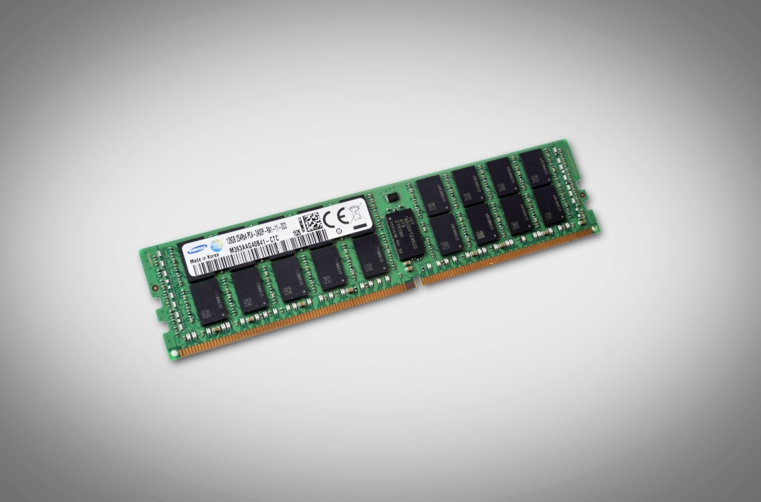
Samsung now mass producing 128GB DDR4 modules using TSV interconnect technology

Samsung on Thursday revealed it is now mass producing memory modules boasting the largest capacity and the highest energy efficiency of any DRAM module. The 128GB DDR4 sticks in question were made possible by utilizing the through silicon via (TSV) interconnect technique.
Foregoing traditional wire bonding, the TSV technique involves grinding chips down to a few dozen micrometers, piercing them with hundreds of tiny holes and vertically connecting them with electrodes passing through the holes. Although not new, the advanced circuitry does allow for a significant boost in signal transmission.
The 128GB modules are comprised of 144 DDR4 chips arranged into 4GB DRAM packages (18 per side for a total of 36), each containing four 20nm 8Gb chips. Samsung says the modules have a special design in which the master chip of each 4GB package embeds the data buffer function, further optimizing performance and power consumption.
The end result is a module that offers speeds of up to 2,400Mbps which is nearly twice the performance and half the power usage as the previous highest capacity DRAM modules, 64GB LRDIMMs.
Samsung said the previous capacity king was hampered by power and speed limitations due to its use of conventional wire bonding.
As you’ve likely surmised by now, these modules are designed for enterprise server and data center applications.
Samsung said it plans to roll out a complete lineup of TSV DRAM modules over the next several weeks in addition to boosting data transfer speeds up to 3,200Mbps.
Comments
Post a Comment